BGA · Substrate · Advanced Packaging
Semiconductor & IC Packaging
Micron-scale drilling, BGA solder-mask windowing and substrate depaneling — critical steps behind modern IC packaging supported by HOYAN LASER micromachining platforms.
Challenges
What this sector demands
Micron-hole arrays with zero conductor damage
Selective removal of solder-mask over BGA pads
Non-contact cutting for brittle substrates
Repeatability across 200 mm and 300 mm formats
Processes
How HOYAN LASER answers
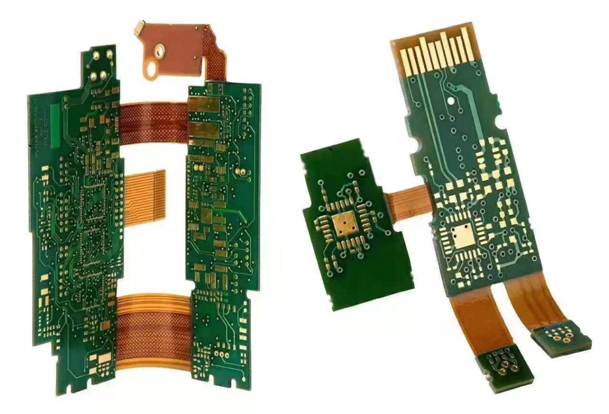
BGA solder-mask opening
UV nanosecond selective ablation with copper protection.
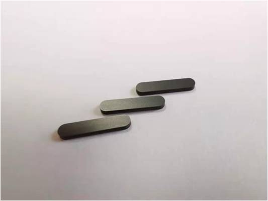
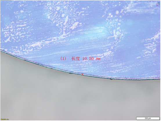
IC substrate depaneling
Green / UV picosecond cutting, zero-taper edges.
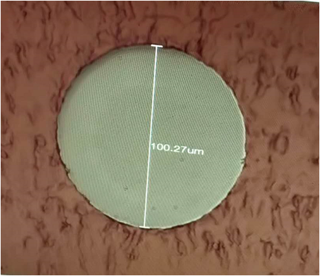
Ceramic micro-hole drilling
Micron array holes on AlN / Al₂O₃ substrates.
Wafer-level QR marking
Roll-to-roll traceability inside the packaging line.
Key metrics
Precision, at a glance
≤ 0.02 mm
Spot size
± 2 µm
Repeat accuracy
0
Recast / HAZ (ps)
24h
Reply SLA
Reference gallery
Real samples from our lab
Recommended platforms
Systems to build this line
Also explore
Other industries

Ready to plan your line?
Free feasibility study, sample cutting and system spec. Reply within one business day.